

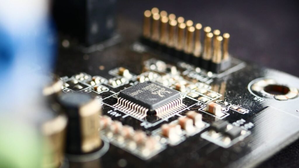
On September 12, Huawei put the Mate XT 2 on sale in China at prices starting around 19,999 yuan, roughly $2,980. Inside it is the Kirin 9050 Pro, which Richard Yu, chairman of Huawei’s consumer business group, called the most powerful Kirin the company has ever built. The more interesting claim was the quieter one: that the chip is entirely free of American technology.
That claim is true in a specific and narrow way, and misleading in a broader one. Both halves matter, because the gap between them is the actual state of China’s semiconductor independence in 2026.
What Huawei actually announced
The headline specification is a nine-core CPU Huawei calls LinxiCore, peaking at 3.1GHz, paired with a Maleoon GPU that now does hardware ray tracing and a Da Vinci NPU that Huawei says runs a 30-billion-parameter mixture-of-experts model entirely on the device. That last number is the one to watch. Running a model that size locally is a memory bandwidth problem as much as a compute problem, and it is the clearest signal of what the chip was designed around.
| Component | What Huawei says it is |
|---|---|
| CPU | Nine-core LinxiCore, peak clock 3.1GHz |
| GPU | Maleoon, with hardware ray tracing added this generation |
| NPU | Da Vinci, running a 30-billion-parameter mixture-of-experts model on device |
| Architecture | LogicFolding, two active silicon layers bonded face to face |
| Vertical interconnects | Around 50 million, at a pitch of roughly 1.5 micrometers |
| Process node | Not disclosed |
| First device | Mate XT 2 tri-fold, on sale in China from September 12, 2026 |
That “not disclosed” line is not an oversight. Huawei has stopped naming process nodes, and for a company whose entire argument is that node names no longer measure the right thing, staying quiet is consistent rather than evasive. It also makes the claims impossible to check without a teardown.
The performance numbers, and the baseline trick
Huawei published two sets of comparisons at launch, and they do not share a baseline. Against the Kirin 9020 in the original Mate XT, it claims a 42 percent overall improvement. Against the newer Kirin 9030 Pro, it claims the three figures below. Quoting the larger headline number against the older chip is a standard move, and it is worth knowing which comparison you are reading.
Huawei’s own figures, presented at launch. No independent verification exists yet.
+24%
+52%
+142%
The graphics figure is the outlier, and the likely explanation is boring: the previous Maleoon had no hardware ray tracing. Adding a fixed-function block to silicon that did not have one produces exactly this kind of jump on the workloads that use it, and nothing at all on the ones that do not.
What LogicFolding actually does
This is the part that matters beyond one phone. Every chipmaker improves density by shrinking transistors, which requires progressively more advanced lithography. Huawei has been cut off from the most advanced lithography, namely ASML’s extreme ultraviolet machines, since 2019. So it stopped trying to shrink and started trying to fold.
LogicFolding splits the logic across two active silicon layers, bonded face to face, connected by roughly 50 million vertical interconnects at about a 1.5 micrometer pitch. Signals that used to travel a long way sideways across the surface of a die now travel a very short way up and down between layers. Shorter paths mean lower resistance and lower capacitance, which means Huawei can drop the operating voltage while raising the density.
The theory behind it has a name. At IEEE ISCAS in Shanghai on May 25, 2026, He Tingbo, president of Huawei’s semiconductor business, presented what Huawei calls the Tau scaling law, proposing that the industry stop optimizing for transistor geometry and start optimizing for tau, the time a signal takes to travel. By that measure, progress no longer requires smaller transistors. It requires shorter distances. Huawei’s stated target is chips with density equivalent to a 1.4 nanometer process by 2031, without ever running a 1.4 nanometer process.
So is it actually free of American technology?
Split the question in two, because Huawei’s claim and the counterargument are answering different halves of it.
Designing a chip and manufacturing one are two different supply chains
The chip architecture, designed in house at Huawei.
A prototype EDA program from Peking University’s School of Integrated Circuits, built to handle 3D layout natively.
Verification on Empyrean Technology’s domestic platform.
Fabrication at SMIC rather than TSMC or Samsung.
ASML lithography scanners, Dutch, deep ultraviolet rather than extreme ultraviolet.
Etch and deposition equipment from Applied Materials and Lam Research, both American, acquired before the 2022 restrictions took effect.
No domestic replacement for either category exists at production scale today.
Read that way, Huawei’s statement is defensible. There is no American intellectual property inside the design. It is also incomplete, because a chip that no American tool touched would need a fab built from machines that do not yet exist in China, and SMIC’s lines are full of equipment bought while it still could buy it. That equipment ages, and it cannot be serviced or replaced through the same channels.
Why this is a bigger deal than one tri-fold phone
The Kirin 9050 Pro is the first real end-to-end test of whether a Chinese design ecosystem can function without Western tooling: a university EDA prototype, a domestic verification platform, and SMIC’s 7nm-class process, working in sequence to produce a shipping product. Huawei says it has designed and mass-produced 381 chips on the Tau principle over six years. This is the first one whose architecture depends on the idea.
The manufacturing side already had a data point. When TechInsights tore down the Kirin 9030 from the Mate 80 Pro Max in December 2025, it confirmed SMIC’s N+3 process, an evolution of the 7nm-class node, reached with no EUV anywhere in the flow. Later analysis of the Kirin 9030 Pro found a minimum metal pitch of 32.5 nanometers, slightly tighter than Intel’s 18A, achieved through self-aligned quadruple patterning, which means running older lithography four times where a modern fab would run EUV once. It works. It is expensive, and yield is the price.
What it means for the phone in your pocket
If you are not buying a Chinese flagship, the direct effect this year is none. Huawei phones are not sold through US carriers, Google services are absent, and the Mate XT 2 costs about $2,980. We went through that device in detail when Huawei launched its second tri-fold a few days after Samsung abandoned its own.
The indirect effect is more interesting, and it runs through the rest of the industry. Huawei is not alone in building its own silicon to reduce exposure to foreign suppliers. Xiaomi made the same argument with a different set of components, which we covered in the piece on its XRing chip and Chinese memory. If a vertically integrated Chinese stack turns out to be viable at volume, the pricing pressure eventually reaches everyone, including Qualcomm’s flagship Snapdragon line, which is currently splitting itself in two partly to manage cost.
There is also a technical possibility worth keeping an eye on. If folding logic vertically really does buy meaningful density without advanced lithography, that is useful to every chipmaker, not only the sanctioned one. The companies with EUV access would get the gain on top of everything they already have.
Frequently asked questions
What is the Kirin 9050 Pro?
Huawei’s flagship mobile processor, announced in September 2026 and shipping first in the Mate XT 2 tri-fold. It has a nine-core LinxiCore CPU peaking at 3.1GHz, a Maleoon GPU with hardware ray tracing, and a Da Vinci NPU that Huawei says runs a 30-billion-parameter model on device. It is the first commercial chip built on the LogicFolding architecture.
Is the Kirin 9050 Pro really free of US technology?
The design is. Huawei’s architecture, a Peking University EDA prototype, Empyrean’s verification platform and SMIC’s fab replace what would normally be American and Western tools. The manufacturing equipment is not. SMIC uses ASML scanners and older Applied Materials and Lam Research machines bought before 2022.
What is LogicFolding?
A chip design method that stacks logic across two bonded silicon layers inside one die rather than laying it out flat, connected by roughly 50 million vertical interconnects. Shorter signal paths lower resistance and capacitance, which raises density and efficiency without needing smaller transistors.
How is LogicFolding different from chiplets?
Chiplets bond separately manufactured dies into a package after each has been designed in two dimensions. LogicFolding designs a single die as one three-dimensional space from the start, which requires design software that most of the industry does not currently have.
What process node is the Kirin 9050 Pro built on?
Huawei did not say. Its predecessors used SMIC’s N+3, a 7nm-class process refined without EUV lithography. Confirming the node on this chip requires a physical teardown, and none has been published.
Can you buy the Kirin 9050 Pro outside China?
Not readily. It debuted in the Mate XT 2, which went on sale in China on September 12, 2026 starting around 19,999 yuan. Huawei phones are not sold through US carriers and ship without Google services.
Does this mean China has caught up in chips?
No. It means the gap is narrowing on design and architecture while remaining wide on manufacturing equipment. SMIC’s best process is still behind leading TSMC and Samsung nodes, and it gets there by running older machines more times per wafer, which costs more and yields less.
The bottom line
Huawei made a precise claim and let everyone else round it up. No American technology sits inside the Kirin 9050 Pro’s design, and that is a real achievement built on a university toolchain and a domestic fab. American and European machines still sit in the building where it was made, and no amount of architectural cleverness changes that in the next few years.
What LogicFolding does change is the question being asked. For thirty years the measure of a chip company was how small it could go. Huawei cannot go smaller, so it is arguing that the measure was wrong, and it has now shipped a product that stands or falls on the argument. The teardown that settles it will arrive within weeks, and it will be worth more than anything either government says in the meantime.
About this article: GeekBlog covers U.S. technology news, AI, phones, smartwatches and gaming. Every story is written and checked under our Editorial Policy. Spotted a mistake or have a story tip? Contact our editors.
